Before the invention of transistors, electronic devices used vacuum tubes, which powered radio, radar, telephones, and early computers. That said, these precursor technologies had significant disadvantages, which limited their widespread adoption.
The semiconductor industry was born in 1947, when William Shockley, John Bardeen, and Walter Brattain invented the first transistor. Initially, they invented the point of contact transistor. William Shockley advanced the technology further by inventing the bipolar junction transistor in 1951. The transistor was a game-changing technology. This technology made vacuum tube near obsolete and allowed for electronic devices to become significantly smaller.
Example products: military components, portable radios, and telephone switching equipment.
Source: Simon-Kucher, “The 1950’s—Laying the Groundwork”
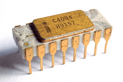
Texas Instruments’ Jack Kilby and Fairchild Semiconductor’s Robert Noyce independently developed the first integrated circuits in 1958 and 1959, respectively, marking the next major technology advancement. Their innovation enabled the fabrication of multiple transistors on a single microchip. Integrated circuits would further shrink electronic devices and enable an ever-greater number of transistors and thereby increase compute power.
Example products: aerospace and military components, mainframe computers, and telecommunications systems.
For more information, see Simon-Kucher’s The 1960’s—The Decade of Integration.

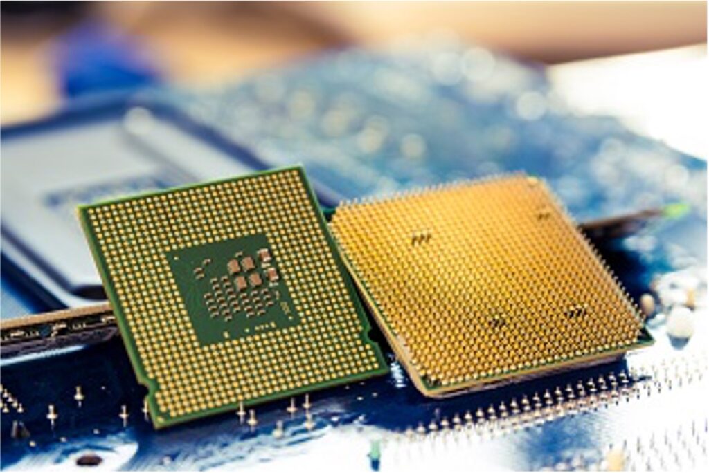
Intel released the world’s first commercial microprocessor in 1971, which integrated thousands of transistors onto a single chip.
The innovation was that a single chip could carry out the function of a larger compute cluster. The microprocessor created the personal computer revolution whereby average individuals and businesses could afford to purchase their own computers. It’s important to note that the power and the capabilities of computers would continue to improve as transistor density improved due to incremental improvements in manufacturing technologies.
Example products: central processing units, Random Access Memory
The next major innovation consolidated the key components of a computer onto a single die. System-on-chip components allowed devices to become significantly smaller by reducing the number of other discrete components needed.
Example products: Smartphones, tablets, IoT and wearable devices, and certain personal computers.
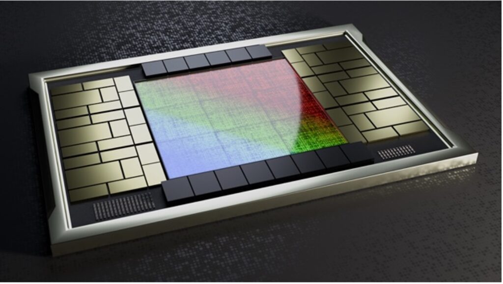
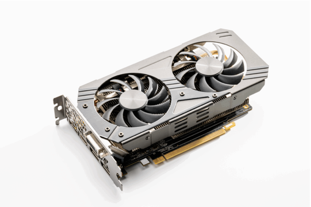
The latest major shift in semiconductor technology is creating a compute paradigm shift away from ultra-low latency serial to higher latency parallel processing. In short, traditional central processing units (CPUs) were inefficient at conducting parallel computation. This spurred the development of purpose-built silicon devices designed for specific tasks.
This marks a profound shift in the semiconductor industry, and we’re now entering a heterogeneous compute landscape where the focus is on designing the chip for the specific task at hand.
Example products: graphics processing units (GPUs), data processing units, and application-specific integrated circuits.
While silicon remains the workhorse, the industry is actively exploring and adopting alternative semiconductor materials to achieve superior performance in specific applications.
For instance, Silicon Carbide (SiC) and Gallium Nitride (GaN) are rapidly gaining prominence in power electronics, particularly for demanding applications like electric vehicles, renewable energy systems, and high-voltage power supplies. Their inherent ability to handle higher power densities, operate at higher temperatures, and switch faster than traditional silicon components leads to significantly improved efficiency and reduced size in power conversion applications.
Beyond incremental improvements to existing designs, leading firms are investing heavily in fundamentally new compute paradigms.

As the semiconductor industry looks ahead, its central challenge is to continuously enhance compute performance despite diminishing returns from traditional scaling. To overcome these hurdles and unlock new capabilities, the industry is pursuing several innovative avenues: